Advertisements
Advertisements
What is the speed of a photon with respect to another photon if (a) the two photons are going in the same direction and (b) they are going in opposite directions?
Concept: undefined >> undefined
Can a photon be deflected by an electric field? Or by a magnetic field?
Concept: undefined >> undefined
Advertisements
A hot body is placed in a closed room maintained at a lower temperature. Is the number of photons in the room increasing?
Concept: undefined >> undefined
Should the energy of a photon be called its kinetic energy or its internal energy?
Concept: undefined >> undefined
In an experiment on photoelectric effect, a photon is incident on an electron from one direction and the photoelectron is emitted almost in the opposite direction. Does this violate the principle of conservation of momentum?
Concept: undefined >> undefined
It is found that yellow light does not eject photoelectrons from a metal. Is it advisable to try with orange light or with green light?
Concept: undefined >> undefined
It is found that photosynthesis starts in certain plants when exposed to sunlight, but it does not start if the plants are exposed only to infrared light. Explain.
Concept: undefined >> undefined
The threshold wavelength of a metal is λ0. Light of wavelength slightly less than λ0 is incident on an insulated plate made of this metal. It is found that photoelectrons are emitted for some time and after that the emission stops. Explain.
Concept: undefined >> undefined
If an electron has a wavelength, does it also have a colour?
Concept: undefined >> undefined
Planck's constant has the same dimensions as
Concept: undefined >> undefined
Two photons of
Concept: undefined >> undefined
Let nr and nb be the number of photons emitted by a red bulb and a blue bulb, respectively, of equal power in a given time.
Concept: undefined >> undefined
The equation E = pc is valid
Concept: undefined >> undefined
The work function of a metal is hv0. Light of frequency v falls on this metal. Photoelectric effect will take place only if
Concept: undefined >> undefined
Light of wavelength λ falls on a metal with work-function hc/λ0. Photoelectric effect will take place only if
Concept: undefined >> undefined
When stopping potential is applied in an experiment on photoelectric effect, no photoelectric is observed. This means that
Concept: undefined >> undefined
If the frequency of light in a photoelectric experiment is doubled, the stopping potential will ______.
Concept: undefined >> undefined
A point source of light is used in a photoelectric effect. If the source is removed farther from the emitting metal, the stopping potential
Concept: undefined >> undefined
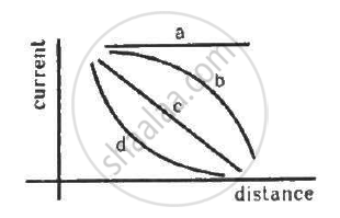
A point source causes photoelectric effect from a small metal plate. Which of the following curves may represent the saturation photocurrent as a function of the distance between the source and the metal?
Concept: undefined >> undefined
When the intensity of a light source in increased,
(a) the number of photons emitted by the source in unit time increases
(b) the total energy of the photons emitted per unit time increases
(c) more energetic photons are emitted
(d) faster photons are emitted
Concept: undefined >> undefined
