Advertisements
Advertisements
Question
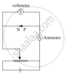
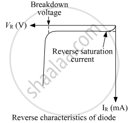
Draw the circuit arrangement for studying the V-I characteristics of a p-n junction diode in reverse bias. Plot the V-I characteristics in this case.
Advertisements
Solution 1

Solution 2
circuit arrangement for studying the V-I characteristics of a p-n junction diode in reverse bias:

V-I characteristics graph of a p-n junction diode in reverse bias:

RELATED QUESTIONS
Meeta's father was driving her to school. At the traffic signal, she noticed that each traffic light was made of many tiny lights instead of a single bulb. When Meeta asked this question to her father, he explained the reason for this.
Answer the following questions based on above information:
(i) What were the values displayed by Meeta and her father?
(ii) What answer did Meeta's father give?
(iii) What are the tiny lights in traffic signals called and how do these operate?
With what considerations in view, a photodiode is fabricated? State its working with the help of a suitable diagram.
Even though the current in the forward bias is known to be more than in the reverse bias, yet the photodiode works in reverse bias. What is the reason?
Draw V − I characteristics of a p-n junction diode. Answer the following questions, giving reasons:
(i) Why is the current under reverse bias almost independent of the applied potential up to a critical voltage?
(ii) Why does the reverse current show a sudden increase at the critical voltage?
Name any semiconductor device which operates under the reverse bias in the breakdown region.
Draw the circuit diagram of a full wave rectifier using p-n junction diode.
Explain its working and show the output, input waveforms.
What happens to the width of depletion player of a p-n junction when it is (i) forward biased, (ii) reverse biased?
Draw the circuit diagram of an illuminated photodiode in reverse bias. How is photodiode used to measure light intensity?
Draw the V-I characteristics of an LED. State two advantages of LED lamps over convertional incandescent lamps.
Draw solar cell V-I characteristics.
Consider the following statements (A) and (B) and identify the correct answer.
- A Zener diode is connected in reverse bias when used as a voltage regulator.
- The potential barrier of the p-n junction lies between 0.1 V to 0.3 V.
The value of power dissipated across the Zener diode (Vz = 15 V) connected in the circuit as shown in the figure is x × 10–1 watt. The value of x, to the nearest integer, is ______.

