Advertisements
Advertisements
प्रश्न
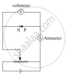
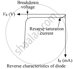
Draw the circuit arrangement for studying the V-I characteristics of a p-n junction diode in reverse bias. Plot the V-I characteristics in this case.
Advertisements
उत्तर १

उत्तर २
circuit arrangement for studying the V-I characteristics of a p-n junction diode in reverse bias:

V-I characteristics graph of a p-n junction diode in reverse bias:

संबंधित प्रश्न
Describe, with the help of a circuit diagram, the working of a photodiode.
How is a photodiode fabricated?
The current in the forward bias is known to be more (~mA) than the current in the reverse bias (~μA). What is the reason, then, to operate the photodiode in reverse bias?
Draw the circuit diagram of a full wave rectifier using p-n junction diode.
Explain its working and show the output, input waveforms.
Describe briefly, with the help of a diagram, the role of the two important processes involved in the formation of a p-n junction.
Write the important considerations which are to be taken into account while fabricating a p-n junction diode to be used as a Light Emitting Diode (LED). What should be the order of the band gap of an LED, if it is required to emit light in the visible range? Draw a circuit diagram and explain its action.
A p-n photodiode is fabricated from a semiconductor with a band gap of 2.5 eV. lt can detect a signal of wavelength ______.
In Figure, assuming the diodes to be ideal ______.

If the resistance R1 is increased (Figure), how will the readings of the ammeter and voltmeter change?

The value of power dissipated across the Zener diode (Vz = 15 V) connected in the circuit as shown in the figure is x × 10–1 watt. The value of x, to the nearest integer, is ______.

