Advertisements
Advertisements
Question
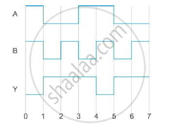
The following figure shows the input waveforms (A, B) and the output waveform (Y) of a gate. Identify the gate, write its truth table and draw its logic symbol.

Advertisements
Solution
The truth table for the gate can be obtained from the waveforms (from t = 1) as
| A | B |
`Y=bar(AB)` |
| 0 | 0 | 1 |
| 0 | 1 | 1 |
| 1 | 0 | 1 |
| 1 | 1 | 0 |
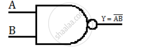
Therefore, from the truth table, we can say that the gate is a NAND gate. The logic symbol for the NAND gate is

APPEARS IN
RELATED QUESTIONS
The logic gate which produces LOW output when one of the input is HIGH and produces
HIGH output only when all of its inputs are LOW is called _______.
(A) AND gate
(B) OR gate
(C) NOR gate
(D) NAND gate
Write the truth table for circuit given in figure below consisting of NOR gates and identify the logic operation (OR, AND, NOT) which this circuit is performing.

(Hint: A = 0, B = 1 then A and B inputs of second NOR gate will be 0 and hence Y=1. Similarly work out the values of Y for other combinations of A and B. Compare with the truth table of OR, AND, NOT gates and find the correct one.)
Give the truth table and circuit symbol for NAND gate
What will be the values of input A and B for the Boolean expression `overline ((A +B) .(A*B)) =1?`
Why is the linear portion of the triode characteristic chosen to operate the triode as an amplifier?
The amplification factor of a triode operating in the linear region depends strongly on ____________ .
Show the variation of voltage with time, for a digital signal.
You are given circuit as shown in the figure, which consists of NAND gate. Identify the logic operation carried out by the two. Write the truth table. Identify the gates equivalent to the tow circuits.

In potential barrier development in a junction diode opposes
A logic gate circuit has two inputs A and B and output Y. The voltage waveforms of A, B and Y are shown below.

The logic gate circuit is ______.
