Advertisements
Advertisements
Question
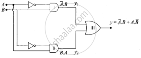
An X-OR gate has following truth table:
| A | B | Y |
| 0 | 0 | 0 |
| 0 | 1 | 1 |
| 1 | 0 | 1 |
| 1 | 1 | 0 |
It is represented by following logic relation `Y = barA.B + A.barB`. Build this gate using AND, OR and NOT gates.
Advertisements
Solution
X-OR gate can be realized by the combination of two NOT gates, two AND gates and one OR gate. According to the problem, the logic relation for the given truth table is
When `Y = barA * B + A * barB = Y_1 + Y_2`
`Y_1 = A * B` and `Y_2 = A * barB`
Y1 can be obtained as output of AND gate 1 for which one input is of A through NOT gate and another input is of B. Y2 can be obtained as the output of AND pate II for which one input is of A and the other input is of B through NOT gate.
Now Y can be obtained as output from OR gate, where Y1 and Y2 are inputs of OR gate.
Thus, the logic circuit of this relation is given below.

APPEARS IN
RELATED QUESTIONS
Which logic gate corresponds to the truth table given below?
|
A |
B |
Y |
|
0 |
0 |
I |
|
0 |
1 |
0 |
|
1 |
0 |
0 |
|
1 |
1 |
0 |
You are given the two circuits as shown in following figure. Show that circuit
- acts as OR gate while the circuit
- acts as AND gate.
(a)

(b)

Write the truth table for a NAND gate connected as given in the following figure.

Hence identify the exact logic operation carried out by this circuit
Draw the schematic symbols for AND, OR, NOT and NAND gate
Answer the following question :
Distinguish between digital and analogue signals.
You are given a circuit below. Write its truth table. Hence, identify the logic operation carried out by this circuit. Draw the logic symbol of the gate it corresponds to.

The following figure shows the input waveforms (A, B) and the output waveform (Y) of a gate. Identify the gate, write its truth table and draw its logic symbol.

Let \[X = A \overline{ BC} + B\overline{ CA} + C\overline{AB } .\] Evaluate X for A = B = C = 0.
Design a logical circuit using AND, OR and NOT gates to evaluate \[A \overline { BC } + B \overline{ CA }\] .
The amplification factor of a triode operating in the linear region depends strongly on ____________ .
Why are NOR gates considered as universal gates?
Show the variation of voltage with time, for a digital signal.
You are given circuit as shown in the figure, which consists of NAND gate. Identify the logic operation carried out by the two. Write the truth table. Identify the gates equivalent to the tow circuits.

A radar is sending out pules of 1 micro second duration at interval of 100 micro-second. The range of the radar is
A CE amplifier has a voltage gain 50, an input impedance of 1000 ohm 1 and an output impedance of 200 ohm. The power gain of the amplifier will be
Which logic gate is similar to a function of two series switches?
For the given circuit, the input digital signals are applied at terminals A, B, and C. What would be the output at terminal y?


In the logic circuit shown in the figure, if input A and B are 0 to 1 respectively, the output at Y would be 'x'. The value of x is ______.

The output (Y) of the given logic implementation is similar to the output of an/a ______ gate.

