Please select a subject first
Advertisements
Advertisements
Identify the logic gate represented by the circuit as shown and write its truth table.
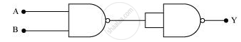
Concept: Digital Electronics and Logic Gates
With the help of circuit diagram explain the working principle of a transistor amplifier as an oscillator.
Concept: Junction Transistor >> Feedback Amplifier and Transistor Oscillator
Distinguish between a conductor, a semiconductor and an insulator on the basis of energy band diagrams.
Concept: Energy Bands in Conductors, Semiconductors and Insulators
The following figure shows the input waveforms (A, B) and the output waveform (Y) of a gate. Identify the gate, write its truth table and draw its logic symbol.
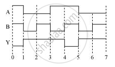
Concept: Digital Electronics and Logic Gates
Draw a circuit diagram to study the input and output characteristics of an n-p-n transistor in its common emitter configuration. Draw the typical input and output characteristics.
Concept: p-n Junction
Explain, with the help of a circuit diagram, the working of n-p-n transistor as a common emitter amplifier.
Concept: p-n Junction
How is a zener diode fabricated so as to make it a special purpose diode? Draw I-V characteristics of zener diode and explain the significance of breakdown voltage.
Explain briefly, with the help of a circuit diagram, how a p-n junction diode works as a half wave rectifier.
Concept: p-n Junction
What will be the values of input A and B for the Boolean expression `overline ((A +B) .(A*B)) =1?`
Concept: Digital Electronics and Logic Gates
Draw a circuit diagram of an n-p-n transistor with its emitter-base junction forward biased and basecollector junction reverse biased. Briefly describe its working.
Explain how a transistor in its active state exhibits a low resistance at its emitter-base junction and high resistance at its base-collector junction.
Concept: Junction Transistor >> Basic Transistor Circuit Configurations and Transistor Characteristics
Derive the expression for the voltage gain of a transistor amplifier in CE configuration in terms of the load resistance RL, current gain a βa and input resistance.
Explain why input and output voltages are in opposite phase.
Concept: Junction Transistor >> Basic Transistor Circuit Configurations and Transistor Characteristics
Write the important considerations which are to be taken into account while fabricating a p-n junction diode to be used as a Light Emitting Diode (LED). What should be the order of band gap of an LED, if it is required to emit light in the visible range? Draw a circuit diagram and explain its action.
Concept: Special Purpose P-n Junction Diodes
Draw the circuit arrangement for studying the output characteristics of n-p-n transistor in CE configuration. Explain how the output characteristics are obtained.
Concept: Transistor Action
Draw a circuit diagram of an n-p-n transistor with its emitter-base junction forward biased and base-collector junction reverse biased. Briefly describe its working.
Explain how a transistor in its active state exhibits a low resistance at its emitter-base junction and high resistance at its base-collector junction.
Concept: Junction Transistor >> Basic Transistor Circuit Configurations and Transistor Characteristics
Derive the expression for the voltage gain of a transistor amplifier in CE configuration in terms of the load resistance RL, current gain βa and input resistance.
Explain why input and output voltages are in the opposite phase.
Concept: Junction Transistor >> Basic Transistor Circuit Configurations and Transistor Characteristics
Write the important considerations which are to be taken into account while fabricating a p-n junction diode to be used as a Light Emitting Diode (LED). What should be the order of the band gap of an LED, if it is required to emit light in the visible range? Draw a circuit diagram and explain its action.
Concept: Special Purpose P-n Junction Diodes
The outputs of two NOT gates are fed to a NOR gate. Draw the logic circuit of the combination of gates. Write its truth table. Identify the gate equivalent to this circuit.
Concept: Digital Electronics and Logic Gates
You are given circuit as shown in the figure, which consists of NAND gate. Identify the logic operation carried out by the two. Write the truth table. Identify the gates equivalent to the tow circuits.
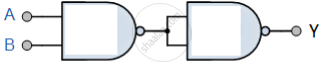
Concept: Digital Electronics and Logic Gates
Answer the following question.
Draw the circuit arrangement for studying the output characteristics of an n-p-n transistor in CE configuration. Explain how the output characteristics is obtained.
Concept: Junction Transistor >> Basic Transistor Circuit Configurations and Transistor Characteristics
What is a solar cell?
Concept: Special Purpose P-n Junction Diodes
You are given a circuit as shown in the figure, which consists of the NAND gate. Identify the logic operation carried out by the two. Write the truth table. Identify the gates equivalent to the tow circuit.
Concept: Digital Electronics and Logic Gates
