Advertisements
Advertisements
प्रश्न
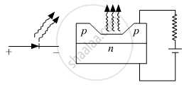
Write the important considerations which are to be taken into account while fabricating a p-n junction diode to be used as a Light Emitting Diode (LED). What should be the order of the band gap of an LED, if it is required to emit light in the visible range? Draw a circuit diagram and explain its action.
Advertisements
उत्तर
For the formation of LED direct bandgap semiconductors like GaAs, CdS, etc should be used which emits light. The p-n junction should be operated in forwarding bias. Most of the Light is produced in p-area of the device so while fabricating LED this area is kept close to the surface of the diode so that the minimum amount of energy is absorbed. One can use different materials for producing different colored Lights. The semiconductor used for the fabrication of visible LEDs must at least have a bandgap of 1.8 eV. The order of the band gap if it is required to emit light in the visible range is about 3 eV to 1.8 eV.

APPEARS IN
संबंधित प्रश्न
Write briefly the important processes that occur during the formation of p−n junction. With the help of necessary diagrams, explain the term 'barrier potential'.
Why is zener diode fabricated by heavily doping both p- and n-sides of the junction?
The current in the forward bias is known to be more (~mA) than the current in the reverse bias (~μA). What is the reason, then, to operate the photodiode in reverse bias?
Describe briefly, with the help of a diagram, the role of the two important processes involved in the formation of a p-n junction.
How does a light emitting diode (LED) work? Give two advantages of LED’s over the conventional incandescent lamps.
Draw the circuit arrangement for studying the V-I characteristics of a p-n junction diode in reverse bias. Plot the V-I characteristics in this case.
Which one of the following is not the advantage of LED?
Consider the following statements (A) and (B) and identify the correct answer.
- A Zener diode is connected in reverse bias when used as a voltage regulator.
- The potential barrier of the p-n junction lies between 0.1 V to 0.3 V.
In Figure, assuming the diodes to be ideal ______.

Briefly explain how emf is generated in a solar cell.
