Advertisements
Advertisements
The wavelength λ of a photon and the de-Broglie wavelength of an electron have the same value. Show that energy of a photon in (2λmc/h) times the kinetic energy of electron; where m, c and h have their usual meaning.
Concept: Wave Nature of Matter
Describe briefly how the Davisson-Germer experiment demonstrated the wave nature of electrons.
Concept: Wave Nature of Matter
Define the terms (i) ‘cut-off voltage’ and (ii) ‘threshold frequency’ in relation to the phenomenon of photoelectric effect.
Using Einstein’s photoelectric equation shows how the cut-off voltage and threshold frequency for a given photosensitive material can be determined with the help of a suitable plot/graph.
Concept: Einstein’s Photoelectric Equation: Energy Quantum of Radiation
Write two characteristic features observed is photoelectric effect which supports the photon pictures of electromagnetic radiation ?
Concept: Photoelectric Effect - Hallwachs’ and Lenard’s Observations
Draw a graph between the frequency of incident radiation (υ) and the maximum kinetic energy of the electrons emitted from the surface of a photosensitive material state clearly how this graph can be used to determine (i) Planck’s constant and (ii) work function of the material.
Concept: Photoelectric Effect - Hallwachs’ and Lenard’s Observations
Plot a graph to show the variation of stopping potential with frequency of incident radiation in relation to photoelectric effect.
Concept: Photoelectric Effect and Wave Theory of Light
How does one explain the emission of electrons from a photosensitive surface with the help of Einstein’s photoelectric equation?
Concept: Einstein’s Photoelectric Equation: Energy Quantum of Radiation
The stopping potential in an experiment on photoelectric effect is 1.5V. What is the maximum kinetic energy of the photoelectrons emitted? Calculate in Joules.
Concept: Photoelectric Effect and Wave Theory of Light
Answer the following question.
Why is the wave theory of electromagnetic radiation not able to explain the photoelectric effect? How does a photon picture resolve this problem?
Concept: Photoelectric Effect and Wave Theory of Light
Name the factors on which photoelectric emission from a surface depends.
Concept: Electron Emission
An electron is accelerated from rest through a potential difference of 100 V. Find:
- the wavelength associated with
- the momentum and
- the velocity required by the electron.
Concept: Wave Nature of Matter
The energy of a photon of wavelength λ is ______.
Concept: Particle Nature of Light: The Photon
Which of the following graphs correctly represents the variation of a particle momentum with its associated de-Broglie wavelength?
Concept: Wave Nature of Matter
(i) State Bohr's quantization condition for defining stationary orbits. How does the de Broglie hypothesis explain the stationary orbits?
(ii) Find the relation between three wavelengths λ1, λ2 and λ3 from the energy-level diagram shown below.
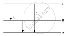
Concept: Bohr’s Model for Hydrogen Atom
In both β− and β+ decay processes, the mass number of a nucleus remains the same, whereas the atomic number Z increases by one in β− decay and decreases by one in β+ decay. Explain giving reason.
Concept: Atomic Spectra
Using Bohr's postulates, derive the expression for the total energy of the electron in the stationary states of the hydrogen atom ?
Concept: Bohr’s Model for Hydrogen Atom
Using Bohr’s postulates for hydrogen atom, show that the total energy (E) of the electron in the stationary states tan be expressed as the sum of kinetic energy (K) and potential energy (U), where K = −2U. Hence deduce the expression for the total energy in the nth energy level of hydrogen atom.
Concept: Bohr’s Model for Hydrogen Atom
Obtain Bohr’s quantisation condition for angular momentum of electron orbiting in nth orbit in hydrogen atom on the basis of the wave picture of an electron using de Broglie hypothesis.
Concept: Bohr’s Model for Hydrogen Atom
Answer the following question.
State Bohr's quantization condition of angular momentum. Calculate the shortest wavelength of the Bracket series and state to which part of the electromagnetic spectrum it belongs.
Concept: De Broglie’s Explanation of Bohr’s Second Postulate of Quantisation
Answer the following question.
Calculate the orbital period of the electron in the first excited state of the hydrogen atom.
Concept: Bohr’s Model for Hydrogen Atom
