Advertisements
Advertisements
प्रश्न
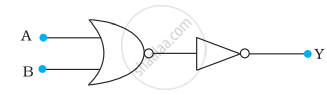
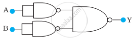
Name the logic gate which generated high output when at least one input is high.
Advertisements
उत्तर
OR Gate :
Y = A + B

` |("A", "B"), (0, 0), (0, 1), (1, 0), (1, 1) | |("Y" = "A" + "B"),(0),(1),(1),(1)|`
APPEARS IN
संबंधित प्रश्न
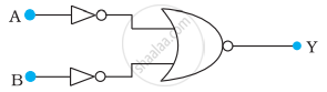
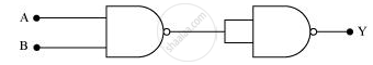
You are given the two circuits as shown in following figure. Show that circuit
- acts as OR gate while the circuit
- acts as AND gate.
(a)
(b)
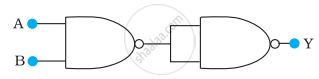
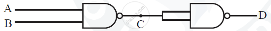
Write the truth table for a NAND gate connected as given in the following figure.
Hence identify the exact logic operation carried out by this circuit
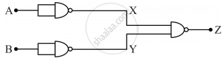
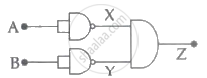
You are given two circuits as shown in following figure, which consist of NAND gates. Identify the logic operation carried out by the two circuits.
(a)
(b)
Give the truth table and circuit symbol for NAND gate
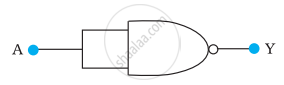
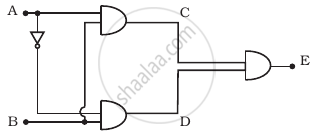
The arrangement given below represents a logic gate :
Copy the following truth table in your answer booklet and complete it showing outputs at C
and D.
| A | B | C | D |
| 0 | 0 | ||
| 1 | 0 | ||
| 0 | 1 | ||
| 1 | 0 |
Answer the following question :
Distinguish between digital and analogue signals.
You are given a circuit below. Write its truth table. Hence, identify the logic operation carried out by this circuit. Draw the logic symbol of the gate it corresponds to.
Identify the logic gate represented by the circuit as shown and write its truth table.
What will be the values of input A and B for the Boolean expression `overline ((A +B) .(A*B)) =1?`
The output of an OR gate is connected to both the inputs of a NAND gate Draw the logic circuit of this combinaion of getes and write its truth table.
Let \[X = A \overline{ BC} + B\overline{ CA} + C\overline{AB } .\] Evaluate X for A = 1, B = 0, C = 1.
Let \[X = A \overline{ BC} + B\overline{ CA} + C\overline{AB } .\] Evaluate X for A = B = C = 0.
Why is the linear portion of the triode characteristic chosen to operate the triode as an amplifier?
Show the variation of voltage with time, for a digital signal.
Draw the truth table of a NOR gate.
The outputs of two NOT gates are fed to a NOR gate. Draw the logic circuit of the combination of gates. Write its truth table. Identify the gate equivalent to this circuit.
The current obtained from a simple filterless rectifier is
A radar is sending out pules of 1 micro second duration at interval of 100 micro-second. The range of the radar is
For the given circuit, the input digital signals are applied at the terminals A, B and C. What would be the output at the terminal y?

Truth table for the given circuit (Figure) is ______.
Draw the output signals C1 and C2 in the given combination of gates (Figure).


An X-OR gate has following truth table:
| A | B | Y |
| 0 | 0 | 0 |
| 0 | 1 | 1 |
| 1 | 0 | 1 |
| 1 | 1 | 0 |
It is represented by following logic relation `Y = barA.B + A.barB`. Build this gate using AND, OR and NOT gates.
In the logic circuit shown in the figure, if input A and B are 0 to 1 respectively, the output at Y would be 'x'. The value of x is ______.

Identify the logic operation carried out by the given circuit:
The given figure shows the waveforms for two inputs A and B and that for the output Y of a logic circuit. The logic circuit is ______.

A logic gate circuit has two inputs A and B and output Y. The voltage waveforms of A, B and Y are shown below.

The logic gate circuit is ______.
Which of the following gives a reversible operation?
