Advertisements
Advertisements
प्रश्न
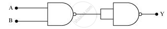
Identify the logic gate represented by the circuit as shown and write its truth table.

Advertisements
उत्तर
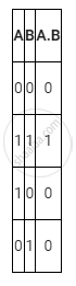
The logic gate represented by the circuit is an AND gate.
The truth table of the AND gate is represented as

APPEARS IN
संबंधित प्रश्न
Draw the schematic symbols for AND, OR, NOT and NAND gate
You are given a circuit below. Write its truth table. Hence, identify the logic operation carried out by this circuit. Draw the logic symbol of the gate it corresponds to.

Let \[X = A \overline{ BC} + B\overline{ CA} + C\overline{AB } .\] Evaluate X for A = B = C = 1.
The amplification factor of a triode operating in the linear region depends strongly on ____________ .
With the help of a diagram, show how you can use several NAND gates to obtain an OR gate.
Useful Constants and Relations :
| 1. Speed of Light in Vacuum | (c) = 3.00 x 10⁸ m/s |
| 2. Charge of a proton | (e) = 1.60 x 10⁻¹⁹C |
| 3. Planck's Constant | (h) = 6.6 x 10⁻³⁴ Js |
| 4. Permeability of vacuum | (μ0) = 4π x 10-7 Hm-1 |
| 5. Electron Volt | (1eV ) = 1.6 x 10 |
| 6. Unified Atomic Mass Unit | (1u) = 931 MeV |
| (π) = 3.14 | |
| ( ln 2 ) = 0.693 |
The current obtained from a simple filterless rectifier is
The output of 2-input or gate is zero only when its
The truth table for the following logic circuit is:

The given figure shows the waveforms for two inputs A and B and that for the output Y of a logic circuit. The logic circuit is ______.
A logic gate circuit has two inputs A and B and output Y. The voltage waveforms of A, B and Y are shown below.

The logic gate circuit is ______.
