Advertisements
Advertisements
Question
You are given two circuits as shown in following figure, which consist of NAND gates. Identify the logic operation carried out by the two circuits.
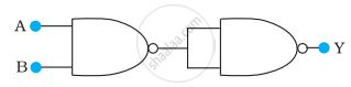
(a)
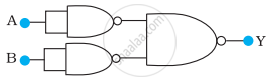
(b)
Advertisements
Solution
In both the given circuits, A and B are the inputs and Y is the output.
a) The output of the left NAND gate will be `bar("A"."B")`, as shown in the following figure.
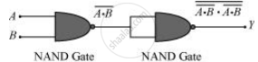
Hence, the output of the combination of the two NAND gates is given as:
`"Y" = bar((bar("A.B")).(bar("A.B")))= bar(bar("AB")) + bar(bar("AB")) = "AB"`
Hence, this circuit functions as an AND gate.
(b) `bar"A"` is the output of the upper left of the NAND gate and `bar"B"` is the output of the lower half of the NAND gate, as shown in the following figure.
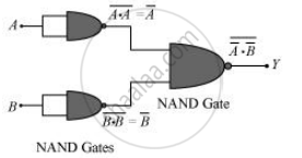
Hence, the output of the combination of the NAND gates will be given as:
`"Y" = bar"A".bar"B" = bar(bar"A") + bar(bar"B") = "A"+"B"`
Hence, this circuit functions as an OR gate.
