Definitions [11]
Intrinsic semiconductors have very low conductivity at room temperature. Therefore, they are not useful for constructing electronic devices. Their electrical conductivity can be increased by adding a suitable impurity. This process is called doping.
The semiconductor to which the dopant is added is called the host.
The impurity added is called a dopant.
A doped semiconductor is called an extrinsic semiconductor or impurity semiconductor.
What is a solar cell?
It is a semiconductor device used to convert photons of solar light into electricity. It generates emf when solar radiation falls on the p-n junction. A p-type silicon wafer of about 300 μm is taken over which a thin layer of n-type silicon is grown on one side by the diffusion process.

A special purpose junction diode that converts light energy into electrical current, works on the principle of the photoelectric effect, operates in reverse bias, and generates a current when exposed to light (proportional to the intensity of incident light), is called a Photodiode.
A unique form of a bipolar device which permits the current flow in the reverse direction when the voltage applied is above a certain characteristic value called Zener voltage or breakdown voltage, most commonly used in voltage regulators to protect other semiconductor devices from fluctuations in voltage, is called a Zener Diode.
With reference to a semiconductor diode, define the depletion region.
A semiconductor diode's depletion zone is the area surrounding the p-n junction where there are no mobile charge carriers, this area generates an electric field that allows the diode to conduct in one direction while blocking in another.
A semiconductor diode is a two-terminal p-n junction device that allows current to pass easily in one direction and offers high resistance in the opposite direction.
In semiconductor physics, what is meant by:
(i) rectifier
(ii) an amplifier
(iii) an oscillator
(i) Rectifier: It is a device which converts alternating current into direct current.
(ii) Amplifier: An amplifier is a device which increases the energy of a weak signal by supplying energy from an external source. An amplifier increases the amplitude of a input signal.
(iii) Oscillator: An oscillator is a device which produces electrical oscillations of adjustable frequency and constant amplitude. An oscillator is basically an amplifier. A part of the output energy is fed back into the L-C circuit to produce sustained oscillations.
With reference to a semiconductor diode, define the potential barrier.
The barrier that the repelling forces use to stop the mobile charge carriers (at the PN junction) is known as the potential barrier.
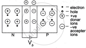
This results from the concentration of immobile charges close to the junction after electrons and holes diffuse across the function.
Formulae [5]
\[R=\frac{V_{IN}-V_{OUT}}{I_Z+I_L}\]
\[I_L=\frac{V_s-V_Z}{R_s}\quad\mathrm{or}\quad I_L=I_S+I_Z\]
\[V_{OUT}=V_{IN}-I_R=V_{IN}-(I_Z+I_L)R\]
\[I_{Z_{max}}=\frac{P_{max}}{V_Z}\]
Where \[P_{max}\] = power dissipation capability of Zener diode.
\[I=I_Z+I_L\]
Key Points
| Aspect | Conductors | Insulators | Semiconductors |
|---|---|---|---|
| Band gap | None (bands overlap) | Large (~10 eV) | Small (~1 eV) |
| Electron transition | Free movement | Not possible easily | Possible with small energy |
| Energy requirement | None | Very high | Low |
| Energy Band Structure | 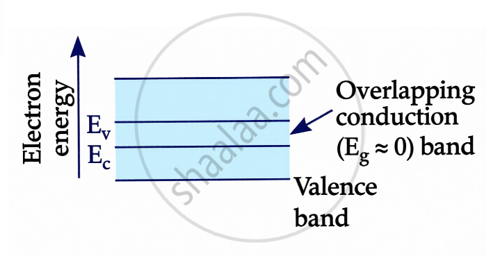 |
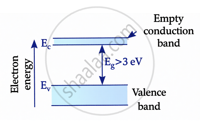 |
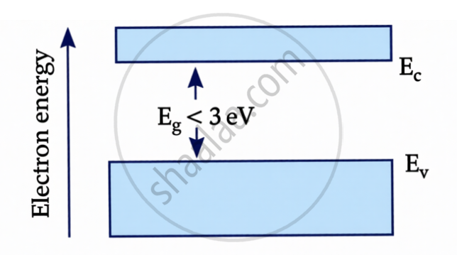 |
- Intrinsic semiconductors have very low conductivity at room temperature.
- Doping increases conductivity.
- A doped semiconductor is called an extrinsic semiconductor.
- The impurity added is called a dopant.
- The semiconductor receiving the impurity is called the host.
- The dopant size should be nearly the same as that of the host atom.
- Pentavalent and trivalent impurities are used as dopants.
- Extrinsic semiconductors are of two types: n-type and p-type.
- A Zener diode maintains a constant voltage across the load as long as the supply voltage is more than the Zener voltage.
- If the input voltage increases, the current through the Zener diode increases while the voltage drop remains constant.
- In the Zener regulator circuit,\[R_s \] is used to limit reverse current through the diode to a safer value \[V_s\], and \[R_s \] is selected so the diode operates in the breakdown region.
- When IZIZ becomes zero, IZIZ reaches its maximum value - at that case \[R=\frac{V_{IN}-V_{OUT}}{I_{Z_{max}}}\].
- Voltage regulator IC (e.g. LM7805) is a special three-terminal device: Pin 1 = \[V_{IN}\], Pin 2 = GND, Pin 3 = +5V regulated output.
- The voltage regulator has been designed to act as an ideal battery.
Important Questions [28]
- If the Charge on the Condenser of 10°F is Doubled, Then the Energy Stored in It Becomes
- Explain the Formation of Energy Band Diagram in Case of Conductor and Semiconductor.
- Distinguish Between Intrinsic and Extrinsic Semiconductor. (Give Any Two Points).
- In a Semiconductor, Acceptor Impurity is
- Distinguish Between P-type and N-type Semiconductors.
- When a Hole is Produced in P-type Semiconductor, There is
- A Pure Semiconductor is ________.
- The Width of Depletion Region of P-n Junction Diode is _______.
- With the Help of a Neat Circuit Diagram, Explain the Working of a Photodiode.
- Colour of Light Emitted by Led Depends Upon
- State its any ‘two’ uses of photodiode.
- Explain the Working of P-n Junction Diode in Forward and Reverse Biased Mode
- With the Help of Neat Labelled Circuit Diagram Explain The Working of Half Wave Rectifier Using Semiconductor Diode.
- What is Zener Diode?
- Describe, with the Help of a Circuit Diagram, the Working of Zener Diode as a Voltage Regulator.
- Explain, with the help of a circuit diagram, the principle and working of a Zener diode as voltage regular.
- When a P-n-p Transistor is Operated in Saturation Region, Then Its
- What Are α And β Parameters for a Transistor? Obtain a Relation Between Them.
- Draw a circuit diagram for studying the input and output characteristics of a n-p-n transistor in common emitter configuration.
- Write the Functions of Three Segments of a Transistor.
- Explain the Working of Transistor as a Switch.
- Explain the Elementary Idea of an Oscillator with the Help of Block Diagram
- In Case of Transistor Oscillator, to Obtain Sustained Oscillations, the Product of Voltage Gain Without Feedback And Feedback Factor Should Be
- Draw the Schematic Symbols for And, Or, Not and Nand Gate
- The Logic Gate Which Produces Low Output When One of the Input is High and Produces High Output Only When All of Its Inputs Are Low is Called
- The Output of Nor Gate is High, When
- Name the Logic Gate Which Generated High Output When at Least One Input is High.
- Which Logic Gate Corresponds to the Truth Table Given Below?
Concepts [12]
- Energy Bands in Materials
- Extrinsic Semiconductor
- Applications of n-type and p-type Semiconductors
- Special Purpose P-n Junction Diodes
- Semiconductor Diode
- Voltage Regulator
- I-V Characteristics of Led
- Transistor and Characteristics of a Transistor
- Transistor as an Amplifier (Ce-configuration)
- Transistor as a Switch
- Oscillators
- Digital Electronics and Logic Gates
