Advertisements
Advertisements
प्रश्न
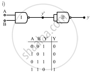
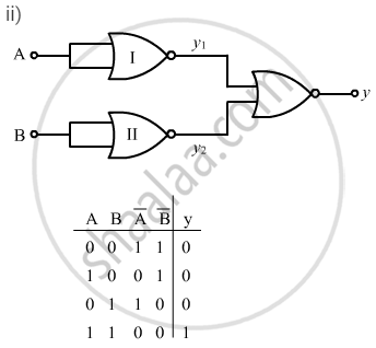
An AND gate can be prepared by repetitive use of
(a) NOT gate
(b) OR gate
(c) NAND gate
(d) NOR gate.
Advertisements
उत्तर
(c) NAND gate
(d) NOR gate


APPEARS IN
संबंधित प्रश्न
You are given the two circuits as shown in following figure. Show that circuit
- acts as OR gate while the circuit
- acts as AND gate.
(a)

(b)

Draw logic symbol of an OR gate and write its truth table.
The following figure shows the input waveforms (A, B) and the output waveform (Y) of a gate. Identify the gate, write its truth table and draw its logic symbol.

The output of an OR gate is connected to both the inputs of a NAND gate Draw the logic circuit of this combinaion of getes and write its truth table.
Let \[X = A \overline{ BC} + B\overline{ CA} + C\overline{AB } .\] Evaluate X for A = B = C = 1.
Let \[X = A \overline{ BC} + B\overline{ CA} + C\overline{AB } .\] Evaluate X for A = B = C = 0.
Design a logical circuit using AND, OR and NOT gates to evaluate \[A \overline { BC } + B \overline{ CA }\] .
(i) Write the truth tables of the logic gates marked P and Q in the given circuit.
(ii) Write the truth table for the circuit.

Show the variation of voltage with time, for a digital signal.
Draw a diagram to show how NAND gates can be combined to obtain an OR gate. (Truth table is not, required)
Useful Constants and Relations:
| 1. | Charge of a proton | (e) | =1.6 × 10⁻¹⁹C |
| 2. | Planck's constant | (h) | = 6·6 × 10-34 Js |
| 3. | Mass of an electron | (m) | = 9·1× 10-31 kg |
| 4. | Permittivity of vacuum | (∈0) | =8 · 85 × 10-12 Fm-1 |
| 5. | `(1/(4pi∈_0))` | =9 ×10⁹ mF-1 | |
| 6. | Permeability of vacuum | (μ0) | = 4π × 10-7 Hm-1 |
| 7. | `((mu_0)/(4pi))` | =1 × 10⁻⁷ Hm-1 | |
| 8. | Speed of light in vacuum | (c) | = 3× 10⁸ ms-1 |
| 9. | Unified atomic mass unit | (u) |
= 931 MeV |
| 10. | Electron volt | (leV) | = 1.6 × 10⁻¹⁹ J |
You are given a circuit as shown in the figure, which consists of the NAND gate. Identify the logic operation carried out by the two. Write the truth table. Identify the gates equivalent to the tow circuit.

The Boolean expression for NAND gate is
A CE amplifier has a voltage gain 50, an input impedance of 1000 ohm 1 and an output impedance of 200 ohm. The power gain of the amplifier will be
Which logic gate is similar to a function of two series switches?
Draw the output signals C1 and C2 in the given combination of gates (Figure).


An X-OR gate has following truth table:
| A | B | Y |
| 0 | 0 | 0 |
| 0 | 1 | 1 |
| 1 | 0 | 1 |
| 1 | 1 | 0 |
It is represented by following logic relation `Y = barA.B + A.barB`. Build this gate using AND, OR and NOT gates.
In the logic circuit shown in the figure, if input A and B are 0 to 1 respectively, the output at Y would be 'x'. The value of x is ______.

A logic gate circuit has two inputs A and B and output Y. The voltage waveforms of A, B and Y are shown below.

The logic gate circuit is ______.
Which of the following gives a reversible operation?
The output (Y) of the given logic gate is similar to the output of an/a:

