Advertisements
Advertisements
Question
Explain the formation of depletion region and barrier potential in PN junction diode.
Advertisements
Solution

Schematic representation

Circuit symbol
1. A p-n junction diode is formed when the p-type semiconductor is fused with an N-type semiconductor.
2. A p-n junction diode is formed when the p-type semiconductor is fused with an N-type semiconductor.
- Forward bias
- Forward bias
a. Forward bias:

- If the positive terminal of the external voltage source is connected to the p-side and the negative terminal to the n-side forward bias takes place.
- Electron moves to n-side holes move to the p side Recombination takes place near the junction and reduces depletion region.
- Electron from n-side accelerates towards p side it experiences reduced potential barrier at the junction.
- Applied voltage is increased, the width of the depletion region and barrier potential further reduced.
- So a large number of electrons pass through the junction.
b. Reverse bias:

- If the positive terminal of the external voltage source is connected to the p-side and the negative terminal to the n-side reverse bias takes place.
- Depletion region is increased potential barrier is also increased.
- Majority of charge carriers from both sides experience a great barrier to cross the junction. So diffusion current reduces.
- The current flows under reverse bias are called reverse saturation current Is.
APPEARS IN
RELATED QUESTIONS
The barrier potential of a silicon diode is approximately, ____________.
Which one of the following represents forward bias diode?
Draw the input and output waveforms of a full wave rectifier.
Distinguish between avalanche breakdown and Zener breakdown.
What is meant by biasing?
Define barrier potential.
Draw the circuit diagram of a half wave rectifier and explain its working.
What is an LED? Give the principle of its operation with a diagram.
Write notes on the photodiode.
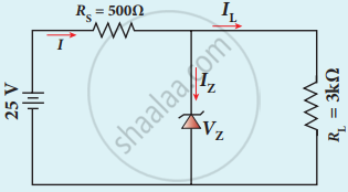
In the given figure of a voltage regulator, a Zener diode of breakdown voltage 10 V is employed. Determine the current through the load resistance, the total current and the current through the diode. Use diode approximation.