Advertisements
Advertisements
प्रश्न
Explain the formation of depletion region and barrier potential in PN junction diode.
Advertisements
उत्तर

Schematic representation

Circuit symbol
1. A p-n junction diode is formed when the p-type semiconductor is fused with an N-type semiconductor.
2. A p-n junction diode is formed when the p-type semiconductor is fused with an N-type semiconductor.
- Forward bias
- Forward bias
a. Forward bias:

- If the positive terminal of the external voltage source is connected to the p-side and the negative terminal to the n-side forward bias takes place.
- Electron moves to n-side holes move to the p side Recombination takes place near the junction and reduces depletion region.
- Electron from n-side accelerates towards p side it experiences reduced potential barrier at the junction.
- Applied voltage is increased, the width of the depletion region and barrier potential further reduced.
- So a large number of electrons pass through the junction.
b. Reverse bias:

- If the positive terminal of the external voltage source is connected to the p-side and the negative terminal to the n-side reverse bias takes place.
- Depletion region is increased potential barrier is also increased.
- Majority of charge carriers from both sides experience a great barrier to cross the junction. So diffusion current reduces.
- The current flows under reverse bias are called reverse saturation current Is.
APPEARS IN
संबंधित प्रश्न
The zener diode is primarily used as ____________.
The barrier potential of a p-n junction depends on
(i) type of semiconductor material
(ii) amount of doping
(iii) temperature
Which one of the following is correct?
A diode is called a unidirectional device. Explain.
What do you mean by leakage current in a diode?
Draw the input and output waveforms of a full wave rectifier.
Write a short note on diffusion current across the p-n junction.
Define barrier potential.
Draw the circuit diagram of a half wave rectifier and explain its working.
Explain the working principle of a solar cell. Mention its applications.
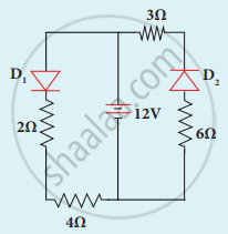
Determine the current flowing through 3 Ω and 4 Ω resistors of the circuit given below. Assume that diodes D1 and D2 are ideal diodes.