English

Differentiate Between Three Segments of a Transistor on the Basis of Their Size and Level of Doping. - Physics

Advertisements
Advertisements

Question

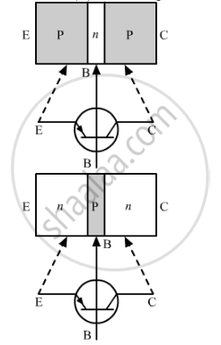
Differentiate between three segments of a transistor on the basis of their size and level of doping.

Advertisements

Solution

Emitter (E) - It is the left hand side thick layer of the transistor, which is heavily doped.

Base (B) - It is the central thin layer of the transistor, which is lightly doped.

Collector (C) - It is the right hand side thick layer of the transistor, which is moderately doped.

shaalaa.com
  Is there an error in this question or solution?
2013-2014 (March) Delhi Set 1

RELATED QUESTIONS

Write clearly, why in the case of a transistor (i) the base is thin and lightly doped


Write clearly, why in the case of a transistor (ii) the emitter is heavily doped.


When a p-n-p transistor is operated in saturation region, then its ______.

(A) base-emitter junction is forward biased and base-collector junction is reverse biased.
(B) both base-emitter and base-collector junctions are reverse biased.
(C) both base-emitter and base-collector junctions are forward biased.
(D) base-emitter junction is reverse biased and base-collector junction is forward biased


Write the functions of the three segments of a transistor.


The figure shows the input waveforms A and B for ‘AND’ gate. Draw the output waveform and write the truth table for this logic gate.


Draw a typical input and output characteristics of an n-p-n transistor in CE configuration. Show how these characteristics can be used to determine (a) the input resistance (r1), and (b) current amplification factor (β)


Draw typical output characteristics of an n-p-n transistor in CE configuration. Show how these characteristics can be used to determine output resistance.


The output characteristic curve of a transistor at constant input current is plotted between


Consider the circuit arrangement shown in figure (a) for studying input and output characteristics of npn transistor in CE configuration.


(a)


(b)

Select the values of RB and RC for a transistor whose VBE = 0.7 V, so that the transistor is operating at point Q as shown in the characteristics shown in figure (b). Given that the input impedance of the transistor is very small and VCC = VBB = 16 V, also find the voltage gain and power gain of the circuit making appropriate assumptions.


If an emitter current is changed by 4 mA, the collector current changes by 3.5 mA. The value of β will be ______.


Share
Notifications

Englishहिंदीमराठी


      Forgot password?
Use app×