मराठी

Using the Necessary Circuit Diagrams, Show How the V-i Characteristics of a P-n Junction Are Obtained in Forward Biasing How Are These Characteristics Made Use of in Rectification? - Physics

Advertisements
Advertisements

प्रश्न

Using the necessary circuit diagrams, show how the V-I characteristics of a p-n junction are obtained in

Forward biasing

How are these characteristics made use of in rectification?

Advertisements

उत्तर

 p-n junction diode under forward bias

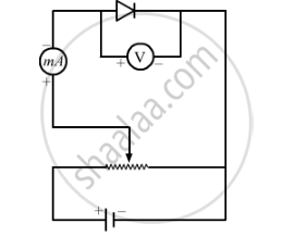
p-side is connected to the positive terminal and n-side to the negative terminal.

Applied voltage drops across the depletion region.

Electron in n-region moves towards the p-n junction and holes in the p-region move towards the junction. The width of the depletion layer decreases and hence, it offers less resistance.

Diffusion of majority carriers takes place across the junction. This leads to the forward current.

The V-I characteristics of p-n junction in forward bias is shown below:

shaalaa.com
  या प्रश्नात किंवा उत्तरात काही त्रुटी आहे का?
2013-2014 (March) Delhi Set 1

व्हिडिओ ट्यूटोरियलVIEW ALL [3]

संबंधित प्रश्‍न

Sunil and his parents were travelling to their village in their car. On the way his mother noticed some grey coloured panels installed on the roof of a low building. She enquired from Sunil what those panels were and Sunil told his mother that those were solar panels.
(a) What were the values displayed by Sunil and his mother? State one value for each.
(b) In what way would the use of solar panels prove to be very useful?
(c) Name the semiconductor device used in solar panels. Briefly explain with the help of a diagram, how this device works


Write briefly the important processes that occur during the formation of p−n junction. With the help of necessary diagrams, explain the term 'barrier potential'.


Draw the circuit diagram of an illuminated photodiode in reverse bias. How is photodiode used to measure light intensity?


The wavelength and intensity of light emitted by a LED depend upon ______.


Explain photodiode.


A p-n photodiode is fabricated from a semiconductor with a band gap of 2.5 eV. lt can detect a signal of wavelength ______.


Read the following paragraph and answer the questions.

LED is a heavily doped P-N junction which under forward bias emits spontaneous radiation. When it is forward-biased, due to recombination of holes and electrons at the junction, energy is released in the form of photons. In the case of Si and Ge diode, the energy released in recombination lies in the infrared region. LEDs that can emit red, yellow, orange, green and blue light are commercially available. The semiconductor used for fabrication of visible LEDs must at least have a band gap of 1.8 eV. The compound semiconductor Gallium Arsenide – Phosphide is used for making LEDs of different colours.


LEDs of different kinds

  1. Why are LEDs made of compound semiconductor and not of elemental semiconductors?
  2. What should be the order of bandgap of an LED, if it is required to emit light in the visible range?
  3. A student connects the blue coloured LED as shown in the figure. The LED did not glow when switch S is closed. Explain why?

    OR
    iii. Draw V-I characteristic of a p-n junction diode in
    (i) forward bias and (ii) reverse bias

How can a photodiode be used to measure light intensity?


What energy conversion takes place in a solar cell?


  1. For a solar-cell the I-V characteristics lies in the (IV) quadrant of the given graph.
  2. In a reverse biased p-n junction diode, the current measured in (μA), is due to majority charge carriers.

Share
Notifications

Englishहिंदीमराठी


      Forgot password?
Use app×