Advertisements
Advertisements
प्रश्न
Define α.
Define the current gain αDC for a transistor.
Advertisements
उत्तर
The dc common-base current ratio or current gain (αdc) is defined as the ratio of the collector current (Ic) to emitter current. (Ig)
`alpha_"dc" = "I"_"C"/"I"_"E"`
संबंधित प्रश्न
In a common-base connection, a certain transistor has an emitter current of 10mA and a collector current of 9.8 mA. Calculate the value of the base current.
Derive the relation between α and β.
Which method of biasing is used for operating a transistor as an amplifier?
In a common base configuration, the transistor has an emitter current of 10 mA and a collector current of 9.8 mA. The value of base current is ______
For a transistor β =75 and IE = 7.5 mA. The value of α is ______
Draw the circuit symbol of the PNP transistor.
Draw the circuit symbol for NPN and PNP transistors. What is the difference in the Emitter, Base, and Collector regions of a transistor?
Draw the circuit diagram to study the characteristic of the transistor in common emitter mode. Draw the input and output characteristics.
The principle based on which a solar cell operates is ____________.
The light emitted in an LED is due to
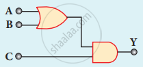
The output of the following circuit is 1 when the input ABC is
Describe the function of a transistor as an amplifier with the neat circuit diagram. Sketch the input and output wave forms.
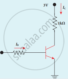
Assuming VCEsat = 0.2 V and β = 50, find the minimum base current (IB) required to drive the transistor given in the figure to saturation.
A transistor having α = 0.8 is connected in common emitter configuration. When the base current changes by 6 mA, then the change in collector current is ______.
For a transistor, the current ratio 'βdc' is defined as the ratio of ______.
In switching circuit, transistor is in ON state. Values of IC and IB are 5.2 mA and 10 µA respectively and value of RC is 1 k`Omega`. If Vcc is at 5.5 V, then VCE is ______.
In switching circuit, transistor is in ON state, values of IE and lB are 10 mA and 0.8 mA respectively and RL is 2 k`Omega`. If VCE is 7.6 V, then VCC is ____________.
In a common emitter amplifier circuit using an n-p-n transistor, the phase difference between the input and the output voltages will be: ____________.
In case of npn transistors, the collector current is always less than the emitter current because ______.
In a silicon transistor, a change of 7.89 mA in the emitter current if produces a change of 7.8 mA in the collector current, then the base current must change by ____________.
In a transistor, the thickness of the base region ____________.
In a transistor, doping level in base is increased slightly, the collector current and base current respectively ______.
In common emitter amplifier, a change of 0.2 mA in the base current causes a change of 5 mA in the collector current. If input resistance is 2K `Omega` and voltage gain is 75, the load resistance used in the circuit is ______.
In a study of transistor as an amplifier, the ratio of collector current to emitter current is 0.98. The collector current is 3mA, then base current will be approximately ______.
A common emitter amplifier has a voltage gain of 50, an input impedance of 100Ω and an output impedance of 2000Ω. The power gain of the amplifier is ______.
A conducting wire has length 'L1' and diameter 'd1'. After stretching the same wire length becomes 'L2' and diameter 'd2' The ratio of resistances before and after stretching is ______.
A common emitter amplifier circuit built using an n-p-n transistor is shown in the figure. Its DC current gain is 300, RC = 4 kΩ and VCC = 20 V. What is the minimum base current for VCE to reach saturation?

Define β
When an n-p-n junction transistor is used as an amplifier in common emitter mode, ______.
In the case of constants ‘α’ and ‘β’ of a transistor ______.
