English

Describe briefly, with the help of a diagram, the role of the two important processes involved in the formation of a p-n junction. - Physics

Advertisements
Advertisements

Questions

Describe briefly, with the help of a diagram, the role of the two important processes involved in the formation of a p-n junction.

Explain, with the help of suitable diagram, the two important processes that occur during the formation of a p-n junction.

Briefly explain the two important processes that occur during the formation of a p-n junction.

Diagram
Explain
Very Long Answer
Advertisements

Solution

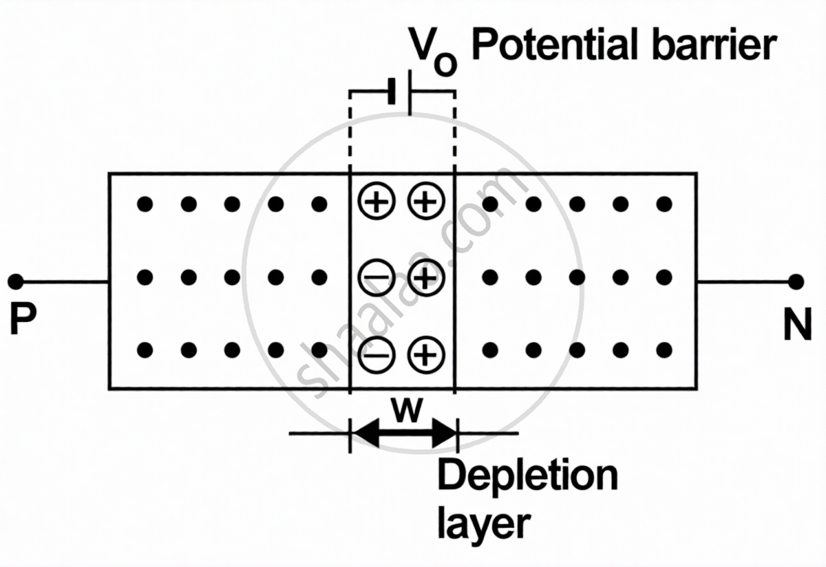
Two major processes that take place during the formation of a p-n junction are diffusion and drift.

Diffusion: In an n-type semiconductor, electrons are present in much higher concentration than holes, whereas in a p-type semiconductor, holes are present in much greater concentration than electrons. When the p-n junction is formed, the difference in concentration causes holes to move from the p-region to the n-region (p → n) and electrons to move from the n-region to the p-region (n → p). This movement of charge carriers across the junction results in the formation of a diffusion current.

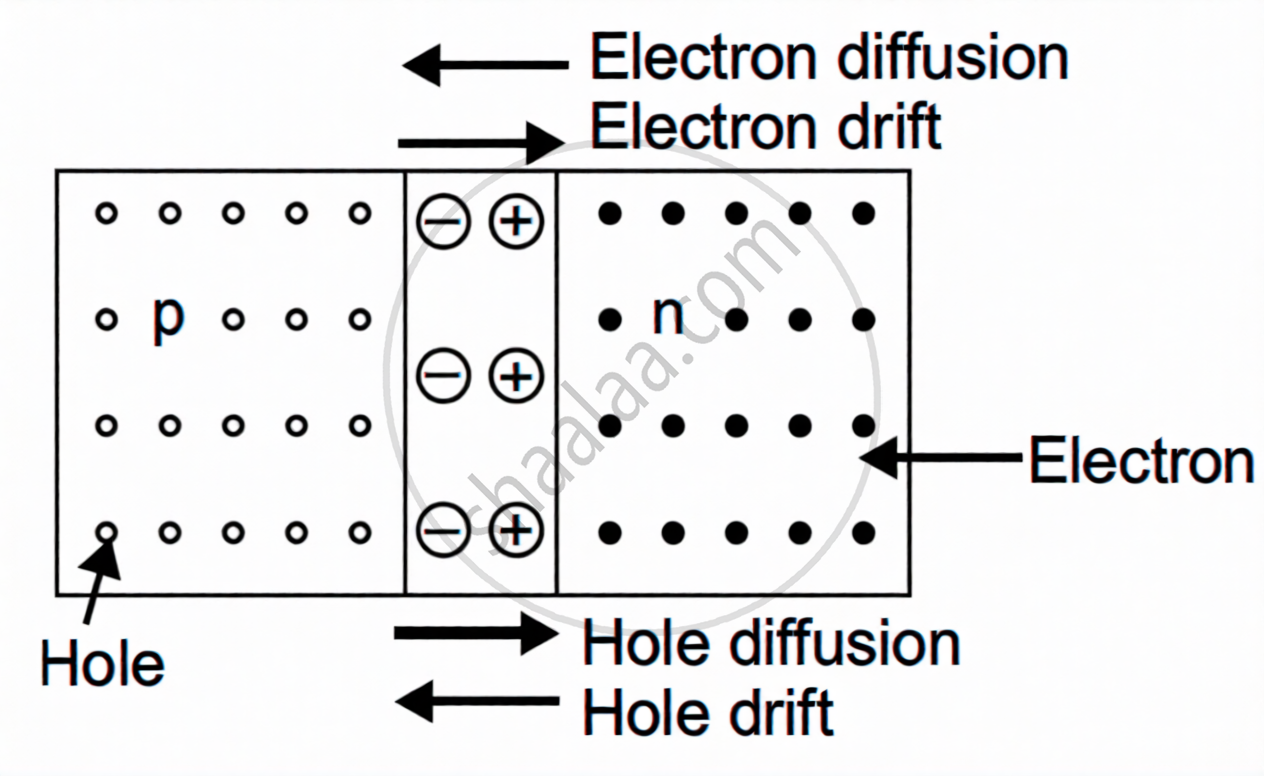
Drift: Drift of charge carriers occurs due to the electric field created at the junction. Because of the built-in potential barrier, an electric field is established from the n-region to the p-region. This electric field causes electrons on the p-side to move toward the n-side and holes on the n-side to move toward the p-side. As a result, a drift current is produced, which flows in the direction opposite to the diffusion current.

shaalaa.com
  Is there an error in this question or solution?
2011-2012 (March) All India Set 1

RELATED QUESTIONS

If a small voltage is applied to a p-n junction diode, how will the barrier potential be affected when it is (i) forward biased


With what considerations in view, a photodiode is fabricated? State its working with the help of a suitable diagram.

Even though the current in the forward bias is known to be more than in the reverse bias, yet the photodiode works in reverse bias. What is the reason?


Carbon, silicon and germanium have four valence electrons each. These are characterised by valence and conduction bands separated by energy band gap respectively equal to (Eg)C, (Eg)Si and (Eg)Ge. Which of the following statements is true?


What happens to the width of depletion player of a p-n junction when it is (i) forward biased, (ii) reverse biased?


Explain the formation of depletion layer and potential barrier in a p−n junction.


The plate resistance of a triode is 8 kΩ and the transconductance is 2.5 millimho. (a) If the plate voltage is increased by 48 V and the grid voltage is kept constant, what will be the increase in the plate current? (b) With plate voltage kept constant at this increased value, by how much should the grid voltage be decreased in order to bring the plate current back to its initial value?


Draw solar cell V-I characteristics.


For LED's to emit light in visible region of electromagnetic light, it should have energy band gap in the range of:


The amplifiers X, Y and Z are connected in series. If the voltage gains of X, Y and Z are 10, 20 and 30, respectively and the input signal is 1 mV peak value, then what is the output signal voltage (peak value)

  1. if dc supply voltage is 10V?
  2. if dc supply voltage is 5V?

Draw solar cells of I-V characteristics.


Share
Notifications

Englishहिंदीमराठी


      Forgot password?
Use app×