Advertisements
Advertisements
Find the speed of an electron with kinetic energy (a) 1 eV, (b) 10 keV and (c) 10 MeV.
Concept: undefined >> undefined
What is the kinetic energy of an electron in electron volts with mass equal to double its rest mass?
Concept: undefined >> undefined
Advertisements
Find the speed at which the kinetic energy of a particle will differ by 1% from its nonrelativistic value \[\frac{1}{2} m_o v^2 .\]
Concept: undefined >> undefined
Define self-inductance of a coil.
Concept: undefined >> undefined
Write the two processes that take place in the formation of a p-n junction.
Concept: undefined >> undefined
Explain two features to distinguish between the interference pattern in Young's double slit experiment with the diffraction pattern obtained due to a single slit.
Concept: undefined >> undefined
A monochromatic light of wavelength 500 nm is incident normally on a single slit of width 0.2 mm to produce a diffraction pattern. Find the angular width of the central maximum obtained on the screen.
Estimate the number of fringes obtained in Young's double slit experiment with fringe width 0.5 mm, which can be accommodated within the region of total angular spread of the central maximum due to single slit.
Concept: undefined >> undefined
A zener diode is fabricated by heavily doping both p- and n- sides of the junction. Explain, why?
Concept: undefined >> undefined
Explain briefly with the help of necessary diagrams, the forward biasing of a p-n junction diode. Also draw characteristic curves.
Concept: undefined >> undefined
Explain briefly with the help of necessary diagrams, the reverse biasing of a p-n junction diode. Also draw characteristic curves.
Concept: undefined >> undefined
The energy levels of an atom are as shown below. Which of them will result in the transition of a photon of wavelength 275 nm?
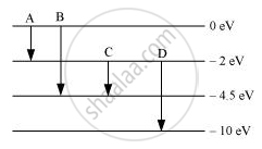
Concept: undefined >> undefined
Which transition corresponds to emission of radiation of maximum wavelength?
Concept: undefined >> undefined
Draw a circuit diagram to study the input and output characteristics of an n-p-n transistor in its common emitter configuration. Draw the typical input and output characteristics.
Concept: undefined >> undefined
Explain, with the help of a circuit diagram, the working of n-p-n transistor as a common emitter amplifier.
Concept: undefined >> undefined
How is a zener diode fabricated so as to make it a special purpose diode? Draw I-V characteristics of zener diode and explain the significance of breakdown voltage.
Explain briefly, with the help of a circuit diagram, how a p-n junction diode works as a half wave rectifier.
Concept: undefined >> undefined
Can we perform Young's double slit experiment with sound waves? To get a reasonable "fringe pattern", what should be the order of separation between the slits? How can the bright fringes and the dark fringes be detected in this case?
Concept: undefined >> undefined
If the separation between the slits in a Young's double slit experiment is increased, what happens to the fringe-width? If the separation is increased too much, will the fringe pattern remain detectable?
Concept: undefined >> undefined
Suppose white light falls on a double slit but one slit is covered by a violet filter (allowing λ = 400 nm). Describe the nature of the fringe pattern observed.
Concept: undefined >> undefined
The slits in a Young's double slit experiment have equal width and the source is placed symmetrically with respect to the slits. The intensity at the central fringe is I0. If one of the slits is closed, the intensity at this point will be ____________ .
Concept: undefined >> undefined
A thin transparent sheet is placed in front of a Young's double slit. The fringe-width will _____________ .
Concept: undefined >> undefined
