Advertisements
Advertisements
प्रश्न
Using the necessary circuit diagrams, show how the V-I characteristics of a p-n junction are obtained in
Reverse biasing
How are these characteristics made use of in rectification?
Advertisements
उत्तर
p-n junction diode under reverse bias

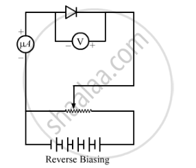
Positive terminal of battery is connected to n-side and negative terminal to p-side.
Reverse bias supports the potential barrier. Therefore, the barrier height increases and the width of depletion region also increases.
Due to the majority carriers, there is no conduction across the junction. A few minority carriers cross the junction after being accelerated by high reverse bias voltage.
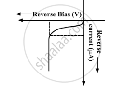
This constitutes a current that flows in opposite direction, which is called reverse current.
The V-I characteristics of p-n junction diode in reverse bias is shown below:

p-n junction diode is used as a half-wave rectifier. Its working is based on the fact that the resistance of p-n junction becomes low when forward biased and becomes high when reverse biased. These characteristics of diode is used in rectification.
APPEARS IN
संबंधित प्रश्न
How is a Zener diode fabricated?
Using the necessary circuit diagrams, show how the V-I characteristics of a p-n junction are obtained in
Forward biasing
How are these characteristics made use of in rectification?
Show the output waveforms (Y) for the following inputs A and B of (i) OR gate (ii) NAND gate ?

The plate resistance of a triode is 8 kΩ and the transconductance is 2.5 millimho. (a) If the plate voltage is increased by 48 V and the grid voltage is kept constant, what will be the increase in the plate current? (b) With plate voltage kept constant at this increased value, by how much should the grid voltage be decreased in order to bring the plate current back to its initial value?
The wavelength and intensity of light emitted by a LED depend upon ______.
What is the magnitude of the potential barrier across a Ge p-n junction?
A p-n photodiode is fabricated from a semiconductor with a band gap of 2.5 eV. lt can detect a signal of wavelength ______.
Read the following paragraph and answer the questions.
|
LED is a heavily doped P-N junction which under forward bias emits spontaneous radiation. When it is forward-biased, due to recombination of holes and electrons at the junction, energy is released in the form of photons. In the case of Si and Ge diode, the energy released in recombination lies in the infrared region. LEDs that can emit red, yellow, orange, green and blue light are commercially available. The semiconductor used for fabrication of visible LEDs must at least have a band gap of 1.8 eV. The compound semiconductor Gallium Arsenide – Phosphide is used for making LEDs of different colours.
|
- Why are LEDs made of compound semiconductor and not of elemental semiconductors?
- What should be the order of bandgap of an LED, if it is required to emit light in the visible range?
- A student connects the blue coloured LED as shown in the figure. The LED did not glow when switch S is closed. Explain why?

OR
iii. Draw V-I characteristic of a p-n junction diode in
(i) forward bias and (ii) reverse bias
Briefly explain how emf is generated in a solar cell.
The value of power dissipated across the Zener diode (Vz = 15 V) connected in the circuit as shown in the figure is x × 10–1 watt. The value of x, to the nearest integer, is ______.


