Advertisements
Advertisements
प्रश्न
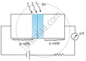
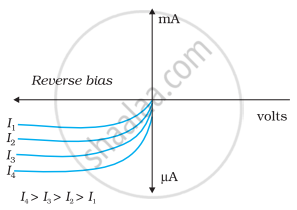
Draw the circuit diagram of an illuminated photodiode and its I-V characteristics.
Advertisements
उत्तर
Illuminated photodiode circuit:

I-V characteristics of photodiode:

APPEARS IN
संबंधित प्रश्न
Using the necessary circuit diagrams, show how the V-I characteristics of a p-n junction are obtained in
Reverse biasing
How are these characteristics made use of in rectification?
A p-n photodiode is fabricated from a semiconductor with band gap of 2.8 eV. Can it detect a wavelength of 6000 nm?
State its any ‘two’ uses of photodiode.
Write the important considerations which are to be taken into account while fabricating a p-n junction diode to be used as a Light Emitting Diode (LED). What should be the order of band gap of an LED, if it is required to emit light in the visible range? Draw a circuit diagram and explain its action.
Explain photodiode.
What is the magnitude of the potential barrier across a Ge p-n junction?
Pressure P varies as P = `alpha/beta "exp" (- (alpha x)/"k"_"BT")`, where x denotes the distance, kB is the Boltzmann's constant, T is the absolute temperature and α and β are constant. The dimension of β is ______.
Consider the following statements (A) and (B) and identify the correct answer.
- A Zener diode is connected in reverse bias when used as a voltage regulator.
- The potential barrier of the p-n junction lies between 0.1 V to 0.3 V.
In Figure, assuming the diodes to be ideal ______.

The value of power dissipated across the Zener diode (Vz = 15 V) connected in the circuit as shown in the figure is x × 10–1 watt. The value of x, to the nearest integer, is ______.

