Advertisements
Advertisements
प्रश्न
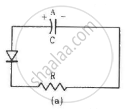
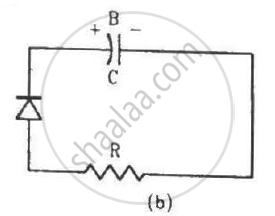
Two identical capacitors A and B are charged to the same potential V and are connected in two circuits at t = 0 as shown in figure. The charges on the capacitors at a time t = CRare, respectively,


विकल्प
VC, VC
VC/e, VC
VC, VC/e
VC/e, VC/e.
Advertisements
उत्तर
In circuit (a), the diode is forward biassed. So, it offers negligible resistance to the flow of current and can thus be replaced by a short circuit. Now, the capacitor charge will leak through the resistance and decay exponentially with time.
Capacitor charge = `(VC)/e`
In circuit (b), the diode is reverse biassed. So, it offers infinite resistance to the current flow and can thus be replaced by an open circuit. As the circuit is open now, no current can flow across the resistance. So, the charge in the capacitor cannot leak through the resistor.
Capacitor charge = VC
APPEARS IN
संबंधित प्रश्न
Distinguish between a metal and an insulator on the basis of energy band diagrams ?
Write two characteristic features to distinguish between n-type and p-type semiconductors ?
How many 1s energy states are present in one mole of sodium vapour? Are they all filled in normal conditions? How many 3s energy states are present in one mole of sodium vapour? Are they all filled in normal conditions?
What is the resistance of an intrinsic semiconductor at 0 K?
Let np and ne be the number of holes and conduction electrons in an intrinsic semiconductor.
A p-type semiconductor is
In a semiconductor,
(a) there are no free electrons at 0 K
(b) there are no free electrons at any temperature
(c) the number of free electrons increases with temperature
(d) the number of free electrons is less than that in a conductor.
The impurity atoms with which pure silicon may be doped to make it a p-type semiconductor are those of
(a) phosphorus
(b) boron
(c) antimony
(d) aluminium.
The band gap between the valence and the conduction bands in zinc oxide (ZnO) is 3.2 eV. Suppose an electron in the conduction band combines with a hole in the valence band and the excess energy is released in the form of electromagnetic radiation. Find the maximum wavelength that can be emitted in this process.
The conductivity of an intrinsic semiconductor depends on temperature as σ = σ0e−ΔE/2kT, where σ0 is a constant. Find the temperature at which the conductivity of an intrinsic germanium semiconductor will be double of its value at T = 300 K. Assume that the gap for germanium is 0.650 eV and remains constant as the temperature is increased.
(Use Planck constant h = 4.14 × 10⁻¹⁵ eV-s, Boltzmann constant k = 8·62 × 10-5 eV/K.)
A semiconducting material has a band gap of 1 eV. Acceptor impurities are doped into it which create acceptor levels 1 meV above the valence band. Assume that the transition from one energy level to the other is almost forbidden if kT is less than 1/50 of the energy gap. Also if kT is more than twice the gap, the upper levels have maximum population. The temperature of the semiconductor is increased from 0 K. The concentration of the holes increases with temperature and after a certain temperature it becomes approximately constant. As the temperature is further increased, the hole concentration again starts increasing at a certain temperature. Find the order of the temperature range in which the hole concentration remains approximately constant.
(Use Planck constant h = 4.14 × 10⁻¹⁵ eV-s, Boltzmann constant k = 8·62 × 10-5 eV/K.)
If the lattice constant of this semiconductor is decreased, then which of the following is correct?

A hole in a. p – type semiconductor is
For germanium crystal, the forbidden gas energy gap
A semiconductor is cooled from T.K to T2K its resistance will
In a common-base circuit calculate the change in the base current if that in the emitter current is αmA and a = 0.98
The valance of an impurity added to germanium crystal in order to convert it into p-type semiconductor is
In a common base configuration Ie = 1 mA α = 0.95 the value of base current is
Three photo diodes D1, D2 and D3 are made of semiconductors having band gaps of 2.5 eV, 2 eV and 3 eV, respectively. Which 0 ones will be able to detect light of wavelength 6000 Å?
The energy required by an electron to jump the forbidden band in silicon at room temperature is about ______.
