Advertisements
Advertisements
प्रश्न
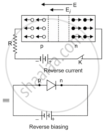
With the help of circuit diagrams, briefly explain the reverse biasing of a p-n junction diode.
आकृती
स्पष्ट करा
Advertisements
उत्तर
The positive terminal of the power supply is connected to the n-type material (cathode), and the negative terminal is connected to the p-type material (anode). This configuration creates an external field that aids the internal field Ei, as shown in the diagram. Under this biasing, the holes in the p-region and the electrons in the n-region are pushed away from the junction, causing the depletion layer to widen and increasing the potential barrier, thus stopping the current flow.
shaalaa.com
या प्रश्नात किंवा उत्तरात काही त्रुटी आहे का?
