मराठी
0
सी. बी. एस. ई.
विज्ञान (इंग्रजी माध्यम) इयत्ता १२
प्रश्नपत्रिका
प्रश्नपत्रिका
३०५१
पाठ्यपुस्तक उत्तरे
४०८२८
MCQ ऑनलाइन सराव परीक्षा
४३
महत्वाचे प्रश्न आणि उत्तरे
२७४३४
संकल्पना स्पष्टीकरण आणि व्हिडिओ
७७५
टाइम टेबल
२५
अभ्यासक्रम
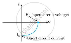
Draw solar cells of I-V characteristics.
Advertisements
Advertisements
प्रश्न
Draw solar cells of I-V characteristics.
आकृती
Advertisements
उत्तर
Show Solution
shaalaa.com
Special Purpose P-n Junction Diodes
त्रुटी नोंदवा
या प्रश्नात किंवा उत्तरात काही त्रुटी आहे का?
Q 5
Q 4
Q 6
2021-2022 (March) Term 2 - Outside Delhi Set 1
APPEARS IN
2021-2022 (March) Term 2 - Outside Delhi Set 1 (with solutions)
Q 5 | 3 marks
Share
0
0
0
0
0
Notifications
Select a course
CANCEL
English
हिंदी
मराठी
user
Login
Create free account
email:
password:
Log in
Forgot password?
Course
विज्ञान (इंग्रजी माध्यम) इयत्ता १२ सी. बी. एस. ई.
घर
इयत्ता १ - ४
इयत्ता ५ - ८
इयत्ता ९ - १०
इयत्ता ११ - १२
प्रवेश परीक्षा
मजकूर किंवा प्रतिमेनुसार शोधा
पाठ्यपुस्तक उत्तरे
अभ्यास साहित्य
सर्व जाहिराती काढून टाका
Change mode
Log out
Use app
×