Advertisements
Advertisements
प्रश्न
Draw the circuit diagram of a half wave rectifier and explain its working.
Explain, with the help of a circuit diagram, the working of a p-n junction diode as a half-wave rectifier.
Advertisements
उत्तर
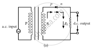
The circuit diagram for a half wave rectifier is shown below:

Working:
During the positive half cycle of the input a.c., the p-n junction is forward biased i.e the forward current flows from p to n and the diode offers a low resistance path to the current. Thus, we get output across-load i.e. a.c input will be obtained as d.c output.
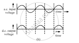
During the negative half cycle of the input a.c., the p-n junction is reversed biased i.e the reverse current flows from n to p, the diode offers a high resistance path to the current. Thus, we get no output across-load. This principle is shown in the diagram given below.

APPEARS IN
संबंधित प्रश्न
Draw the circuit diagram of a full wave rectifier. Explain its working showing its input and output waveforms.
Briefly explain how the output voltage/current is unidirectional.
When the diode shows saturated current, dynamic place resistance is _____________ .
Draw the circuit diagram of a full wave rectifier.
The output of the given circuit in figure is given below.

To reduce the ripples in a rectifier circuit with capacitor filter ______.
- RL should be increased.
- input frequency should be decreased.
- input frequency should be increased.
- capacitors with high capacitance should be used.
Assuming the ideal diode, draw the output waveform for the circuit given in figure. Explain the waveform.

With the help of a circuit diagram, explain briefly how a p-n junction diode works as a half-wave rectifier.
With the help of a circuit diagram, explain how a full wave rectifier gives output rectified voltage corresponding to both halves of the input ac voltage.
Name the device which utilizes the unilateral action of a pn diode to convert ac into dc.
