Advertisements
Advertisements
प्रश्न
Describe the two main types of semiconductors and contrast their conduction mechanism.
Advertisements
उत्तर
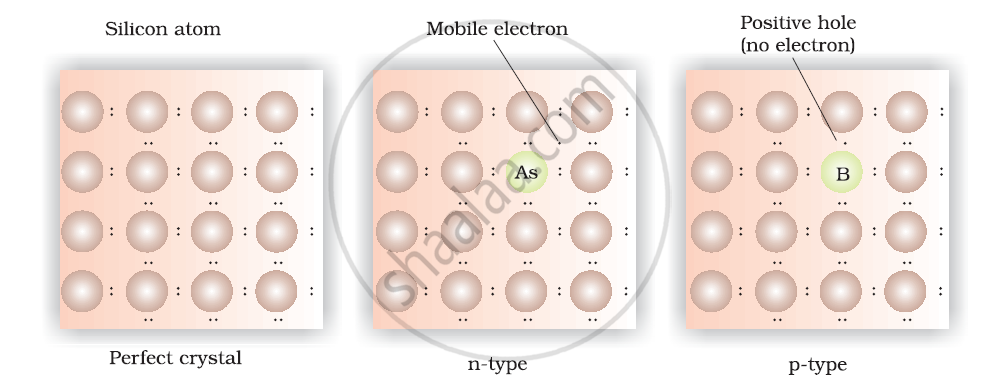
The two main types of semiconductors are:
- n-type semiconductor
- p-type semiconductor
(1) n-type semiconductor:
- The semiconductor whose increased conductivity is a result of negatively charged electrons is called an n-type semiconductor.
- When the crystal of a group 14 element like Si (Silicon) or Ge (Germanium) is doped with a group 15 element like P (Phosphorus) or As (Arsenic), an n-type semiconductor is formed.
- Si and Ge each have four valence electrons.
- In their crystals, each Si or Ge atom forms four covalent bonds.
- P and As contain five valence electrons each.
- When Si or Ge is doped with P or As, these elements take up some of the crystal’s lattice sites.
- Four out of five electrons from P, or As, are used in the formation of covalent bonds with four neighbouring Si or Ge atoms.
- The remaining fifth electron is delocalised, which increases the conductivity of the doped Si or Ge.
(2) p-type semiconductor:
- The semiconductor whose increase in conductivity is a result of an electron hole is called a p-type semiconductor.
- When a crystal of group 14 elements such as Si (Silicon) or Ge (Germanium) is doped with a group 13 element such as B (Boron), Al (Aluminum), or Ga (Gallium) (which contain only three valence electrons), a p-type semiconductor is formed.
- When a Si crystal is doped with B, the three valence electrons are used to form three covalent bonds with neighbouring Si atoms.
- The fourth bond needed to complete the Si’s covalent bonding is missing, creating an electron hole in the lattice.
- An electron from a neighbouring atom can move and fill the electron hole. However, in doing so, it creates an electron hole at its original position.
- This process makes it seem like the electron hole is moving opposite the electron that filled it.
- When an electric field is applied, electrons move toward the positively charged plate through the electron holes.
- It will appear as if the electron holes are positively charged and are moving toward the negatively charged plate.
संबंधित प्रश्न
A group 14 element is to be converted into n-type semiconductor by doping it with a suitable impurity. To which group should this impurity belong?
Classify each of the following as being either a p-type or a n-type semiconductor:
- Ge doped with In
- B doped with Si
Explain the following with suitable examples:
12-16 group compounds
What type of semiconductor is obtained when
Ge is doped with In?
What type of semiconductor is obtained when
Si is doped with P?
Solids with conductivities ranging from 104 to 107 ohm-1 m-1 are ____________.
Semiconductors have conductivity (in ohm-1 m-1) in the range of ____________.
Electrical conductivity of semiconductors increases with increase in ____________.
Which kind of defects are introduced by doping?
Silicon doped with electron-rich impurity forms ______.
Which of the following statements are true about semiconductors?
(i) Silicon doped with electron-rich impurity is a p-type semiconductor.
(ii) Silicon doped with an electron-rich impurity is an n-type semiconductor.
(iii) Delocalised electrons increase the conductivity of doped silicon.
(iv) An electron vacancy increases the conductivity of n-type semiconductor.
Why are solids incompressible?
Why does the electrical conductivity of semiconductors increase with rise in temperature?
Assertion: Semiconductors are solids with conductivities in the intermediate range from 10–6 – 104 ohm–1m–1.
Reason: Intermediate conductivity in semiconductor is due to partially filled valence band.
