Definitions [25]
A basic semiconductor device that controls the flow of electric current in a circuit, which when forward biased behaves as a closed circuit and when reverse biased behaves as an open circuit, is called a p-n Junction Diode.
- The conversion of AC voltage into a DC voltage is called Rectification.
- The process of converting an alternating current into a direct current is called rectification.
- The electronic circuit which rectifies AC voltage is called a Rectifier.
- The device used to convert an alternating current into a direct current is called a rectifier.
- A rectifier that consists of one p-n junction diode in which alternate pulses of AC input are rectified, having a maximum efficiency of 40.6% and output frequency the same as that of input, is called a Half-Wave Rectifier.
- A rectifier which rectifies only one-half of each AC input supply cycle is called a half-wave rectifier.
To rectify AC power for using both half cycles of the sine wave, a different rectification circuit configuration is used, which is known as full-wave rectification.
- A rectifier that consists of two p-n junction diodes in which both the pulses of AC input are rectified, having a maximum efficiency of 81.2% and an output frequency twice that of the input, is called a Full-Wave Rectifier.
- A rectifier which rectifies both halves of each AC input cycle is called a full wave rectifier.
The ratio of the r.m.s. value of the AC component to the value of the DC component in the rectifier output is called the Ripple Factor.
A circuit which removes the AC component (ripple) from the rectified output is called a Filter Circuit.
A unique form of a bipolar device which permits the current flow in the reverse direction when the voltage applied is above a certain characteristic value called Zener voltage or breakdown voltage, most commonly used in voltage regulators to protect other semiconductor devices from fluctuations in voltage, is called a Zener Diode.
What is a solar cell?
It is a semiconductor device used to convert photons of solar light into electricity. It generates emf when solar radiation falls on the p-n junction. A p-type silicon wafer of about 300 μm is taken over which a thin layer of n-type silicon is grown on one side by the diffusion process.

A special purpose junction diode that converts light energy into electrical current, works on the principle of the photoelectric effect, operates in reverse bias, and generates a current when exposed to light (proportional to the intensity of incident light), is called a Photodiode.
A device that converts light energy into electricity through the photovoltaic effect, absorbs sunlight and generates electric current as electrons are knocked loose from atoms, is called a Solar Cell or Photovoltaic Cell.
A special purpose junction diode that emits light when electric current passes through it, works in forward biased mode, and whose wavelength of light emitted depends on the semiconductor materials used, is called a Light Emitting Diode (LED).
Define peak value of alternating signal.
The maximum value of an alternating current or emf in either direction is known as the peak value.
A junction transistor which is a semiconductor device having two junctions and three terminals, in which the current is carried by both electrons and holes (hence the name Bipolar), is called a Bipolar Junction Transistor.
A transistor configuration in which the collector of the transistor is common to both the input and the output is called the Common Collector (CC) Configuration.
A transistor configuration in which the emitter of the transistor is common to both the input and the output is called the Common Emitter (CE) Configuration.
A transistor configuration in which the base of the transistor is common to both the input and the output is called the Common Base (CB) Configuration.
A transistor in which a p-type semiconductor (base) layer separates two layers of the n-type semiconductor (emitter and collector), and in whose circuit symbol the arrow is drawn from base pointing towards emitter, is called an n-p-n Transistor.
A transistor in which an n-type semiconductor (base) layer separates two layers of the p-type semiconductor (emitter and collector), and in whose circuit symbol the arrow is drawn from emitter pointing towards base, is called a p-n-p Transistor.
Define α.
The dc common-base current ratio or current gain (αdc) is defined as the ratio of the collector current (Ic) to emitter current. (Ig)
`alpha_"dc" = "I"_"C"/"I"_"E"`
Define β
The dc common-emitter current ratio or current gain (βdc) is defined as the ratio of the collector current (IC) to base current (IB).
`beta_"dc" = "I"_"C"/"I"_"B"`
A signal that has only two states (0 and 1) is called a Digital Signal.
A device that acts as a building block for digital circuits and performs basic logical functions that are fundamental to digital circuits is called a Logic Gate.
A signal that has continuous values is called an Analog Signal.
Formulae [6]
Ripple Factor = \[\frac {\text {r.m.s. value of AC component}}{\text {value of DC component}}\]
\[\alpha_{ac} = \dfrac{\Delta I_C}{\Delta I_E}\]
αdc = \[\frac {I_C}{I_E}\] (value lies between 0.95 to 0.99)
\[\beta_{ac} = \dfrac{\Delta I_C}{\Delta I_B}\]
βdc = \[\frac {I_C}{I_B}\] (always > 1)
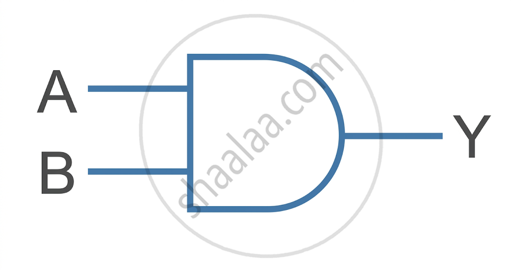
| AND Gate | Y = A ⋅ B |
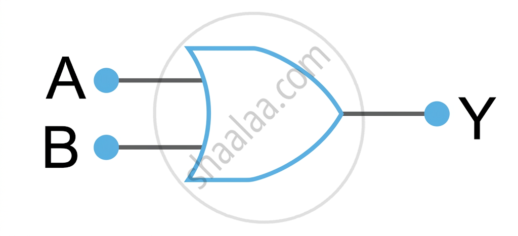
| OR Gate | Y = A + B |
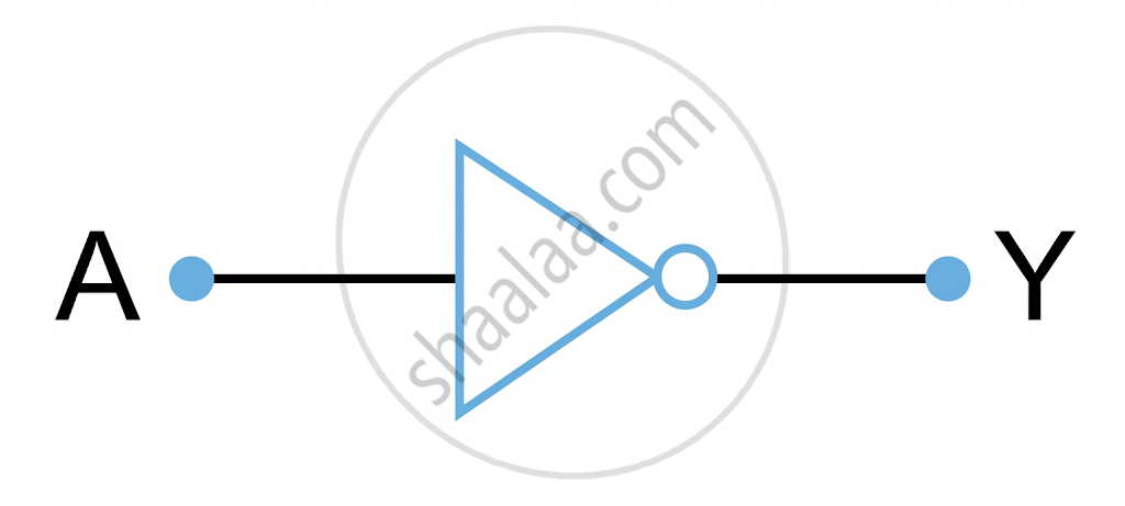
| NOT Gate | Y = \[\overline A\] |
| NAND Gate | Y = \[\overline {AB}\] |
| NOR Gate | Y= \[\overline {(A+B)}\] |
| X-OR Gate | Y = A ⊕ B = \[\overline A\] ⋅ B + \[\overline {AB}\] |
Key Points
- Size & Weight: Semiconductor devices are smaller in size and lightweight, which also enables faster speed of operation.
- Power Consumption: They operate at small voltages (few mV) and require very less current (µA or mA), hence consume lesser power and produce almost no heating effects — making them thermally stable.
- Controllability: The electronic properties of semiconductors can be controlled to suit our requirement, and fabrication of ICs is possible.
- Sensitivity: They are sensitive to electrostatic charges, radiation, and fluctuations in temperature — making them fragile in harsh environments.
- Limitations: They are not useful for controlling high power, require controlled conditions for manufacturing, and very few materials are semiconductors.
- A rectifier is a circuit which converts an AC supply into a unidirectional DC supply.
- A p-n junction diode acts as a rectifier because it allows current to flow in one direction only.
- The bridge rectifier circuit uses semiconductor diodes for converting AC, as it allows current to flow in one direction only.
- Input to the rectifier is AC \[(V_{IN})\]; output is DC \[(V_{OUT})\] — shown as a full-wave rectified signal.
- Rectification is the fundamental principle behind power supply circuits in electronic devices.
- A half-wave rectifier uses a single diode, allowing current to flow in one direction, with an AC power source\[V_{ac}\] connected to the diode and a resistor in series.
- Output is discontinuous and pulsating DC - only positive half cycles appear across the load.
- Alternative (negative) half cycles of the AC supply go to waste, making efficiency very low.
- The output waveform shows only the positive side of the sinusoidal cycle, clamping off the negative side.
- Circuit components: transformer (primary & secondary), single diode, and load resistor \[R_L\].
- A transformer is used to step up or step down the AC voltage before rectification.
- A full-wave rectifier rectifies both half-cycles of the AC input; the output is continuous and pulsating.
- Two types: Centre-tap rectifier (uses 2 diodes) and Bridge rectifier (uses 4 diodes).
- The output of a full-wave rectifier is continuous but pulsating — it can be made smooth using a filter circuit.
- A large capacitor in parallel with the output load resistor reduces the ripple from the rectification process.
- Full-wave rectifiers are used in power supplies to convert AC voltages to DC voltages.
- A bridge rectifier uses no centre-tap transformer, making it more commonly used in practice.
- For a transistor operating as an amplifier in CE configuration, the E-B junction is forward biased while the C-B junction is reverse biased.
- The AC current gain (βac) is the ratio of small change in collector current (ΔIC) to small change in base current (ΔIB) at constant VCE. The DC current gain (βdc) is the ratio of IC to IB, which is always greater than 1.
- The Voltage Gain (Av) is the ratio of change in output voltage (ΔVo) to change in input voltage (ΔVi). The Power Gain is the ratio of change in output power (ΔPo) to change in input power (ΔPi).
- In output characteristics, IC is independent of VCE as long as the collector-emitter junction is reverse biased. IC is large for large values of IB when VCE is constant.
| OR GATE | NOT GATE | AND GATE | NOR GATE | NAND GATE |
|---|---|---|---|---|
 |
 |
 |
 |
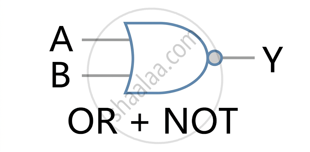 |
| 2 inputs, 1 output | 1 input, 1 output | 2 inputs, 1 output | 2 inputs, 1 output | 2 inputs, 1 output |
| Y = A + B | Y = Ā | Y = A·B | Y = (A + B)̅ | Y = (A·B)̅ |
| If any input is high, output is high | Inverted input is produced | If any input is low, output is low | When both inputs are low, output is high | When both inputs are high, output is low |
Concepts [10]
- Basics of Semiconductor Devices
- p-n Junction Diode as a Rectifier
- Half Wave Rectifier
- Full Wave Rectifier
- Ripple Factor
- Filter circuits
- Special Purpose P-n Junction Diodes
- Applications of semiconductors : Rectifier diode, LED, Zener diode, Photo diode, Photovoltaic cell, BJT, FET, SCR., MOSFET
- Bipolar Junction Transistor (BJT)
- Logic Gates
