Advertisements
Advertisements
प्रश्न
Write the truth table for the circuits given in following figure consisting of NOR gates only. Identify the logic operations (OR, AND, NOT) performed by the two circuits.
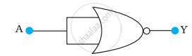
(a)
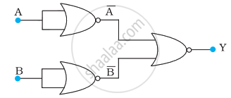
(b)
Advertisements
उत्तर
(a) A acts as the two inputs of the NOR gate and Y is the output, as shown in the following figure. Hence, the output of the circuit is `bar(A+A)`.
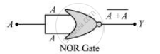
The truth table for the same is given as:
| A | Y`(=bar"A")` |
| 0 | 1 |
| 1 | 0 |
This is the truth table of a NOT gate. Hence, this circuit functions as a NOT gate.
(b) A and B are the inputs and Y is the output of the given circuit. By using the result obtained in solution (a), we can infer that the outputs of the first two NOR gates are `barA` and `barB` as shown in the following figure.
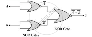
`bar"A" and bar "B"` are the inputs for the last NOR gate. Hence, the output for the circuit can be written as:
`"Y" = bar(bar"A" + bar"B") = bar(bar"A") . bar(bar"B") = "A.B"`
The truth table for the same can be written as:
| A | B | Y (=A⋅B) |
| 0 | 0 | 0 |
| 0 | 1 | 0 |
| 1 | 0 | 0 |
This is the truth table of an AND gate. Hence, this circuit functions as an AND gate.
