Advertisements
Advertisements
प्रश्न
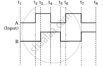
The figure shows the input waveforms A and B for ‘AND’ gate. Draw the output waveform and write the truth table for this logic gate.

Advertisements
उत्तर
Output waveform will be as follows :

Truth table of AND gate :
| A | B | Y |
| 1 | 1 | 1 |
| 1 | 0 | 0 |
| 0 | 1 | 0 |
| 0 | 0 | 0 |
APPEARS IN
संबंधित प्रश्न
What are α and β parameters for a transistor? Obtain a relation between them.
Write clearly, why in the case of a transistor (i) the base is thin and lightly doped
Write clearly, why in the case of a transistor (ii) the emitter is heavily doped.
Differentiate between three segments of a transistor on the basis of their size and level of doping.
How is a transistor biased to be in active state?
Write the functions of the three segments of a transistor.
Draw a typical input and output characteristics of an n-p-n transistor in CE configuration. Show how these characteristics can be used to determine (a) the input resistance (r1), and (b) current amplification factor (β)
Draw typical output characteristics of an n-p-n transistor in CE configuration. Show how these characteristics can be used to determine output resistance.
The output characteristic curve of a transistor at constant input current is plotted between
If an emitter current is changed by 4 mA, the collector current changes by 3.5 mA. The value of β will be ______.
