Advertisements
Advertisements
प्रश्न
Draw a typical input and output characteristics of an n-p-n transistor in CE configuration. Show how these characteristics can be used to determine (a) the input resistance (r1), and (b) current amplification factor (β)
Advertisements
उत्तर
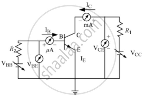
CE configuration is the most widely used transistor.

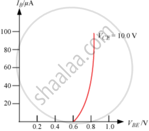
Variation of base current (IB) with the base-emitter voltage VBE is called input characteristics.
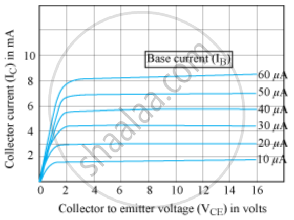
Variation of collector current IC with the collector − Emitter voltage VCE is called output characteristics
Input characteristics

Output characteristics

Parameters of Transistors
Input resistance (ri)
`r_i = ((triangleV_"BE")/(triangleI_B))_(V_"CE")`
ΔVBE − Base-emitter voltage
ΔIB − Base current
VCE − Constant collector-emitter voltage
Output resistance (r0)
`r_0 = ((triangleV_"CE")/(triangleI_C))_(I_B)`
ΔVCE − Collector-emitter voltage
ΔIC − Collector current
IB − Base current
Current amplification factor (β)
`beta_(ac) = ((triangleI_c)/(triangleI_B))_(V_(CE))`
IC − Collector current
IB − Base current
VCE − Constant collector-emitter voltage.
APPEARS IN
संबंधित प्रश्न
What are α and β parameters for a transistor? Obtain a relation between them.
Write clearly, why in the case of a transistor (i) the base is thin and lightly doped
Write clearly, why in the case of a transistor (ii) the emitter is heavily doped.
Differentiate between three segments of a transistor on the basis of their size and level of doping.
When a p-n-p transistor is operated in saturation region, then its ______.
(A) base-emitter junction is forward biased and base-collector junction is reverse biased.
(B) both base-emitter and base-collector junctions are reverse biased.
(C) both base-emitter and base-collector junctions are forward biased.
(D) base-emitter junction is reverse biased and base-collector junction is forward biased
Write the functions of the three segments of a transistor.
The figure shows the input waveforms A and B for ‘AND’ gate. Draw the output waveform and write the truth table for this logic gate.

Draw typical output characteristics of an n-p-n transistor in CE configuration. Show how these characteristics can be used to determine output resistance.
The output characteristic curve of a transistor at constant input current is plotted between
Sanya performed an experiment of obtaining characteristic curves of a junction diode. When she forward biased it, she found that beyond forward voltage V = Vk, the conductivity is very high. When she reverse biased the diode she found that a very small current (of about a few microamperes) flows in the diode. It remained constant even though she varied the voltage.
(i) In Figure 1 below, which one of the diodes is forward biased?

Figure 1
(ii) What is meant by a saturation current?
(iii) When applied voltage during forward bias is small, why does no current flow in the diode?
(iv) The circuit shown in Figure 2 below contains two diodes, each with a forward resistance of 50 Ω and with infinite resistance during reverse bias. If the battery voltage is 6V, then calculate the current through the 100 Ω resistance.

Figure 2
