Advertisements
Advertisements
प्रश्न
Draw the necessary energy band diagrams to distinguish between conductors, semiconductors and insulators.
How does the change in temperature affect the behaviour of these materials ? Explain briefly.
Write any two distinguishing features between conductors, semiconductors and insulators on the basis of energy band diagrams.
Advertisements
उत्तर १
Conductors: (i) For conductors, the valence band is completely filled and the conduction band can have two possibilities—either it is partially filled with an extremely small energy gap between the valence and conduction bands or it is empty, with the two bands overlapping each other, as shown.
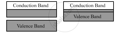
(ii) On applying even an small electric field, conductors can conduct electricity.
Insulators: (i) For insulators, the energy gap between the conduction and valence bands is very large. Also, the conduction band is practically empty, as shown.
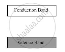
(ii) When an electric field is applied across such a solid, the electrons find it difficult to acquire such a large amount of energy to reach the conduction band. Thus, the conduction band continues to be empty. That is why no current flows through insulators.
Semiconductors: (i) The energy band structure of semiconductors is similar to that of insulators, but in their case, the size of forbidden energy gap is much smaller than that of the insulators, as shown.
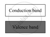
(ii) When an electric field is applied to a semiconductor, the electrons in the valence band find it comparatively easier to shift to the conduction band. So, the conductivity of semiconductors lies between the conductivity of conductors and insulators.
उत्तर २
Energy Band Diagram for a Conductor:
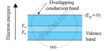
In conductors, the conduction and the valence band overlap each other.
As the temperature increase, the conductivity of the conductors decreases due to increase in the thermal motion of the free electrons.
Energy Band Diagram for an Insulator :
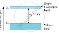
Here, the valence band is completely filled and the conduction band is empty. The energy band gap of the insulator is quite large. So, on increasing the temperature, the electrons of the valence band are not able to reach the conduction band. Therefore, electrical conduction in these materials is impossible.
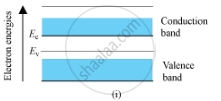
Energy Band Diagram for a Semiconductor
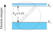
In semiconductors, the valence band is totally filled and the conduction band is empty but the energy gap between conduction band and valence band is quite small. At 0 K, electrons are not able to cross even this small energy gap and, hence, the conduction band remains totally empty. Therefore, the semiconductor at 0 K behaves as an insulator. At room temperature, some electrons in the valence band acquire thermal energy greater than energy band gap, which is less than 3 eV and jump over to the conduction band where they are free to move under the influence of even a small change in the temperature.
